| CPC H01L 23/552 (2013.01) [H01L 21/561 (2013.01); H01L 21/78 (2013.01); H01L 24/13 (2013.01); H01L 2224/13024 (2013.01); H01L 2924/182 (2013.01)] | 4 Claims |
|
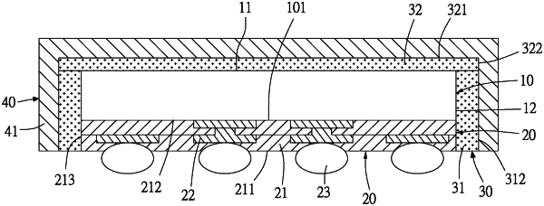
1. An integrated circuit (IC) package structure, comprising:
a chip having an active surface and a bottom surface opposite to the active surface;
a redistribution layer (RDL) structure provided on the chip and be electrically connected thereto;
a molding compound structure provided on outer surfaces of the chip and the RDL structure; and
an electromagnetic interference (EMI) shielding structure provided on outer surfaces of the molding compound structure,
wherein the molding compound structure includes:
a first molding compound layer provided on a plurality of outer side surfaces of the chip and on a plurality of outer side surfaces of the RDL structure; and
a second molding compound layer provided on the bottom surface of the chip and connected to the first molding compound layer,
wherein the EMI shielding structure includes a first EMI shielding layer provided on a plurality of outer side surfaces of the first molding compound layer and on a plurality of outer side surface and a bottom surface of the second molding compound layer; and
wherein the second molding compound layer is formed with a plurality of recesses, the recesses are disposed corresponding to the bottom surface of the chip, and the recesses being filled up by the first EMI shielding layer.
|