| CPC H01L 23/552 (2013.01) [H01L 21/0334 (2013.01); H01L 21/565 (2013.01); H01L 23/3107 (2013.01); H01L 24/13 (2013.01); H01L 2924/15313 (2013.01)] | 23 Claims |
|
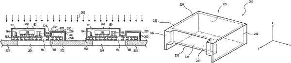
1. A semiconductor device, comprising:
a semiconductor package including,
a substrate comprising a land grid array,
a component disposed over the substrate, and
an encapsulant deposited over the component, wherein the land grid array is disposed outside the encapsulant;
a fanged metal mask disposed over the land grid array, wherein the fanged metal mask includes a front surface oriented toward the encapsulant, a first fang extending from the front surface toward the encapsulant at a first side of the front surface, and a second fang extending from the front surface toward the encapsulant at a second side of the front surface; and
a shielding layer formed over the semiconductor package and fanged metal mask.
|