| CPC H01L 23/552 (2013.01) [H01L 21/568 (2013.01); H01L 23/3107 (2013.01); H01L 23/66 (2013.01); H01L 2223/6677 (2013.01)] | 25 Claims |
|
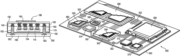
1. A method of making a semiconductor device, comprising:
providing a semiconductor die;
disposing the semiconductor die over a substrate;
depositing an encapsulant over the semiconductor die and substrate;
forming a trench in the encapsulant around the semiconductor die;
forming a shielding layer over the encapsulant and into the trench;
forming an opening in the shielding layer;
disposing a solder bump in the opening;
forming an antenna on the substrate opposite the semiconductor die; and
mounting the semiconductor die to a printed circuit board (PCB) by reflowing the solder bump onto a contact pad of the PCB, wherein the PCB is larger than the substrate.
|