| CPC H01L 23/552 (2013.01) [H01L 23/49822 (2013.01)] | 10 Claims |
|
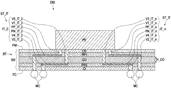
1. An electronic device, comprising:
a support substrate having a mounting face and a connection face opposite to the mounting face;
an electronic integrated circuit chip mounted to the mounting face; and
a matrix of connectors mounted to the connection face;
wherein the support substrate comprises:
an interconnection structure including a pair of conductive interconnection tracks that connect the electronic integrated circuit chip to the matrix of connectors, wherein the pair of conductive interconnection tracks are configured to circulate differential signals, and wherein the pair of conductive interconnection tracks comprises two interconnection tracks extending parallel to the mounting and connection faces and facing each other at different depths of the support substrate while being separated from each other by a dielectric layer of the support substrate; and
a structure for isolating electromagnetic fields configured to be electrically connected to an electrical reference point, the structure comprising at least two pairs of conductive isolation tracks, configured to be electrically connected to the electrical reference point, each pair of the at least two pairs of conductive isolation tracks comprising two isolation tracks extending parallel to the mounting and connection faces and facing each other at different depths of the substrate while being separated from each other by said dielectric layer; and
wherein the pair of conductive interconnection tracks is located between said at least two pairs of conductive isolation tracks and extending parallel to the at least two pairs of conductive isolation tracks.
|