| CPC H01L 23/5389 (2013.01) [H01L 21/563 (2013.01); H01L 21/6835 (2013.01); H01L 23/147 (2013.01); H01L 23/3121 (2013.01); H01L 23/49816 (2013.01); H01L 23/49822 (2013.01); H01L 23/49827 (2013.01); H01L 24/81 (2013.01); H01L 24/97 (2013.01); H01L 24/16 (2013.01); H01L 25/0652 (2013.01); H01L 2221/68345 (2013.01); H01L 2224/73203 (2013.01); H01L 2224/73204 (2013.01); H01L 2224/81001 (2013.01); H01L 2224/81801 (2013.01); H01L 2224/97 (2013.01); H01L 2924/01013 (2013.01); H01L 2924/01029 (2013.01); H01L 2924/01032 (2013.01); H01L 2924/01033 (2013.01); H01L 2924/01047 (2013.01); H01L 2924/01074 (2013.01); H01L 2924/01078 (2013.01); H01L 2924/01079 (2013.01); H01L 2924/01082 (2013.01); H01L 2924/01322 (2013.01); H01L 2924/014 (2013.01); H01L 2924/10329 (2013.01); H01L 2924/14 (2013.01); H01L 2924/15153 (2013.01); H01L 2924/1517 (2013.01); H01L 2924/181 (2013.01); H01L 2924/19041 (2013.01)] | 20 Claims |
|
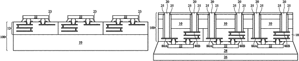
1. A method of forming a device comprising:
providing a substrate substantially free from integrated circuit devices;
forming a first interconnect structure over a first side of the substrate, wherein the first interconnect structure comprises a first metal feature and a second metal feature;
bonding a first die onto the first side of the first interconnect structure;
forming a first through via and a second through via extending through the substrate to the first metal feature and the second metal feature of the first interconnect structure, wherein a first length of the first through via is greater than a second length of the second through via; and
forming a second interconnect structure on a second side of the substrate.
|
|
8. A method comprising:
forming a first interconnect structure over a first side of a substrate, the first interconnect structure comprising a first metal feature and a second metal feature;
etching a first recess and a second recess on a second side of the substrate, the first recess exposing the first metal feature, the second recess exposing the second metal feature;
forming a first through via in the first recess and a second through via in the second recess, the first through via having a different length than the second through via;
forming a second interconnect structure over the second side of the substrate opposite the first side; and
bonding a first die to the second side of the second interconnect structure.
|
|
15. A method of forming a device comprising:
forming a first interconnect structure over a first side of a substrate, wherein the first interconnect structure comprises a first metal feature and a second metal feature, the first metal feature being closer to the substrate than the second metal feature;
bonding a first die to the first interconnect structure;
after bonding the first die to the first interconnect structure, forming a first through via and a second through via extending from a second side of the substrate and into the first interconnect structure, wherein the first through via contacts the first metal feature and has a first length, wherein the second through via contacts the second metal feature and has a second length, wherein the first length is less than the second length; and
forming a second interconnect structure on the second side of the substrate, the second interconnect structure comprising a third metal feature and a fourth metal features, the third metal feature being electrically coupled to the first through via, the fourth metal feature being electrically coupled to the second through via.
|