| CPC H01L 23/5226 (2013.01) [H01L 21/76802 (2013.01); H01L 21/76879 (2013.01); H01L 23/528 (2013.01)] | 20 Claims |
|
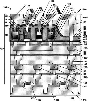
1. An integrated circuit device, comprising:
a semiconductor substrate;
a metal interconnect structure comprising a plurality of metal interconnect layers over the semiconductor substrate;
an array of device structures disposed between two of the plurality of metal interconnect layers, wherein the device structures comprise top electrodes;
a hydrophobic dielectric that fills gaps between the device structures;
an interlayer dielectric disposed above the hydrophobic dielectric;
an interfacial layer between the interlayer dielectric and the hydrophobic dielectric, wherein the interfacial layer has a wafer contact angle (WCA) intermediate between that of the hydrophobic dielectric and that of the interlayer dielectric; and
top electrode vias connecting the top electrodes to conductors within an upper of the two of the plurality of metal interconnect layers, wherein the top electrode vias pass successively through the hydrophobic dielectric, the interfacial layer, and the interlayer dielectric.
|