| CPC H01L 23/5226 (2013.01) [H01L 21/76897 (2013.01); H01L 29/401 (2013.01); H01L 29/41733 (2013.01); H01L 29/4175 (2013.01); H01L 29/66742 (2013.01); H01L 29/0673 (2013.01); H01L 29/42392 (2013.01); H01L 2029/7858 (2013.01); H01L 29/78696 (2013.01)] | 20 Claims |
|
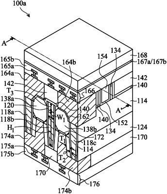
1. A semiconductor device structure, comprising:
a plurality of nanostructures stacked in a vertical direction;
a gate structure formed over the nanostructures;
an S/D structure formed adjacent to the gate structure;
a first via formed adjacent to the S/D structure, wherein a topmost surface of the S/D structure is higher than a topmost surface of the first via, and the first via is filled with a conductive layer;
a first contact structure formed over the S/D structure, wherein a portion of the first contact structure is lower than a top surface of the S/D structure; and
a second contact structure formed below the S/D structure, wherein the first via is in direct contact with the first contact structure and the second contact structure, and
wherein an entirety of the gate structure is higher than an entirety of the first via, and wherein the first contact structure is electrically connected to the second contact structure by the S/D structure or the first via.
|