| CPC H01L 23/49822 (2013.01) [H01L 21/4857 (2013.01); H01L 21/4853 (2013.01); H01L 23/49816 (2013.01); H01L 24/13 (2013.01); H01L 24/16 (2013.01); H01L 2224/13147 (2013.01); H01L 2224/16225 (2013.01)] | 20 Claims |
|
1. An electronic device, comprising:
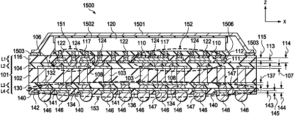
a multilevel package substrate having a first level and a second level, the first level extending in a first plane of orthogonal first and second directions, the second level extending in a second plane of the first and second directions, the second level including a first trace layer with a first conductive trace feature, a conductive first via that contacts the first conductive trace feature, and a first dielectric layer, the first level on the second level and including a second trace layer with a second conductive trace feature, the second conductive trace feature having a first portion and a second portion, the first portion having a first thickness along a third direction, the third direction orthogonal to the first and second directions, the second portion having a side and a second thickness along the third direction, wherein the side of the second portion faces away from the first plane, and the second thickness is greater than the first thickness; and
a die having a conductive terminal electrically coupled to the side of the second portion, wherein the second portion of the second conductive trace feature locates within selective areas of the first level and the selective areas are along a periphery of the die.
|