| CPC H01L 23/481 (2013.01) [H01L 21/76897 (2013.01); H01L 21/76898 (2013.01)] | 20 Claims |
|
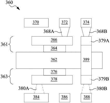
1. A method of making a semiconductor device, comprising:
manufacturing a first transistor over a first side of a substrate;
depositing a spacer material against a sidewall of the first transistor;
recessing the spacer material to expose a first portion of the sidewall of the first transistor;
manufacturing a first electrical connection to the transistor, a first portion of the first electrical connection contacts a surface of the first transistor farthest from the substrate, and a second portion of the first electrical connection contacts the first portion of the sidewall of the first transistor; and
manufacturing a self-aligned interconnect structure (SIS) extending along the spacer material, wherein the spacer material separates a portion of the SIS from the first transistor, and the first electrical connection directly contacts the SIS.
|