| CPC H01L 23/481 (2013.01) [H01L 21/486 (2013.01); H01L 21/76879 (2013.01)] | 20 Claims |
|
1. A method of forming a semiconductor device, comprising:
providing a substrate;
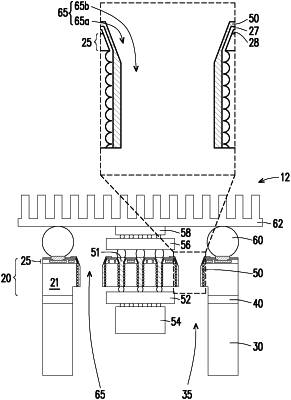
forming at least one via penetrating through the substrate, wherein the at least one via comprises a plurality of concave portions on a sidewall thereof;
forming a liner layer filling in the plurality of concave portions of the at least one via; and
performing a cyclic deposition and etching process to form a conductive layer on the sidewall of the at least one via, covering the liner layer, and extending onto a surface of the substrate, wherein a thickness of the conductive layer on the sidewall of the at least one via is varied.
|