| CPC H01L 23/44 (2013.01) [H05K 7/20236 (2013.01); H01L 2023/405 (2013.01); H01L 2023/4056 (2013.01); H01L 2023/4068 (2013.01); H01L 2023/4087 (2013.01)] | 20 Claims |
|
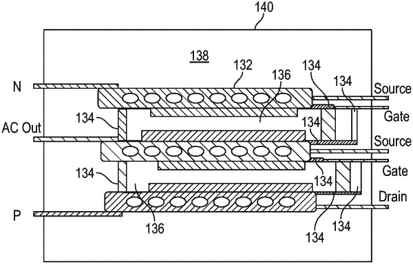
1. A semiconductor package comprising:
one or more power semiconductor die comprised in a die module;
a first heat sink directly coupled to one or more source pads of the die module;
a second heat sink directly coupled to one or more drain pads of the die module;
a gate contact coupled with one or more gate pads of the die module; and
a coating coupled directly to the die module;
wherein the gate contact is configured to extend through an immersion cooling enclosure.
|