| CPC H01L 21/823878 (2013.01) [H01L 21/76224 (2013.01); H01L 21/823807 (2013.01); H01L 21/823864 (2013.01); H01L 21/8249 (2013.01); H01L 27/0623 (2013.01); H01L 29/0649 (2013.01)] | 20 Claims |
|
1. A method of making a semiconductor structure comprising:
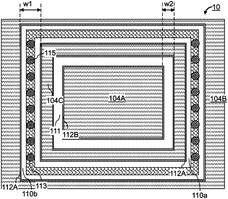
forming at least two moat trenches in a semiconductor device layer, wherein the at least two moat trenches surround a first semiconductor substrate material portion of the semiconductor device layer, and are laterally surrounded by a second semiconductor substrate material portion of the semiconductor device layer, and comprise a first moat trench and a second moat trench;
depositing a conformal diffusion barrier layer in the first moat trench and in the second moat trench;
forming insulating sidewall spacers on sidewalls of the first moat trench while filling the second moat trench with a portion of an insulating sidewall spacer material, wherein the insulating sidewall spacers are laterally spaced apart from each other by a gap that laterally surrounds one of the insulating sidewall spacers and is laterally surrounded by another of the insulating sidewall spacers; and
physically removing a portion of the conformal diffusion barrier layer inside the first moat trench from underneath the gap.
|