| CPC H01L 21/823871 (2013.01) [H01L 21/31111 (2013.01); H01L 21/31116 (2013.01); H01L 21/76802 (2013.01); H01L 21/76877 (2013.01); H01L 21/823821 (2013.01); H01L 23/528 (2013.01); H01L 23/53295 (2013.01); H01L 27/0924 (2013.01); H01L 29/0847 (2013.01); H01L 21/02211 (2013.01); H01L 21/02271 (2013.01); H01L 21/26513 (2013.01); H01L 21/266 (2013.01); H01L 21/31053 (2013.01); H01L 21/76224 (2013.01); H01L 21/823814 (2013.01); H01L 21/823864 (2013.01); H01L 21/823878 (2013.01); H01L 29/66545 (2013.01)] | 20 Claims |
|
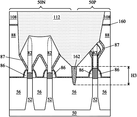
1. A semiconductor device, comprising:
an interlayer dielectric comprising a first material;
a first source/drain region of a first device embedded in the interlayer dielectric;
a second source/drain region of a second device embedded in the interlayer dielectric;
a fin of the first device, wherein the fin is below the first source/drain region and has a longitudinal axis extending in a first direction;
an isolation region comprising a second dielectric material embedded in the interlayer dielectric and disposed between the first device and the second device, wherein a first width of an upper portion of the isolation region within the interlayer dielectric is greater than a second width of a lower portion of the isolation region within the interlayer dielectric in a cross-sectional view along a second direction perpendicular to the first direction, wherein first sidewalls of the upper portion having the first width and second sidewalls of the lower portion having the second width are in physical contact with the interlayer dielectric in the cross-sectional view; and
a contact connected through a first portion of a contact etch stop layer to the first source/drain region and connected through a second portion of the contact etch stop layer to the second source/drain region, the contact etch stop layer comprising a third dielectric material being different from the second dielectric material.
|