| CPC H01L 21/823857 (2013.01) [H01L 21/31105 (2013.01); H01L 21/823412 (2013.01); H01L 21/823431 (2013.01); H01L 21/823437 (2013.01); H01L 21/823462 (2013.01); H01L 21/823821 (2013.01); H01L 27/088 (2013.01); H01L 29/0665 (2013.01); H01L 29/42392 (2013.01); H01L 29/78696 (2013.01)] | 20 Claims |
|
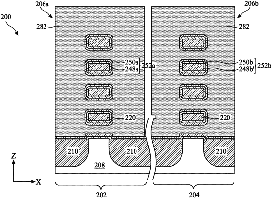
10. A semiconductor device, comprising:
a substrate having a first region and a second region;
a first transistor located in the first region, the first transistor including:
a plurality of first channel members vertically stacked above the substrate, and
a first gate structure wrapping around each of the first channel members, the first gate structure including a first interfacial layer and a first high-k dielectric layer over the first interfacial layer; and
a second transistor located in the second region, the second transistor including:
a plurality of second channel members vertically stacked above the substrate, and
a second gate structure wrapping around each of the second channel members, the second gate structure including a second interfacial layer and a second high-k dielectric layer over the first interfacial layer, wherein the second high-k dielectric layer includes a higher oxygen concentration than the first high-k dielectric layer, and wherein a top portion of the second high-k dielectric layer includes an alloy oxide, a middle portion of the second high-k dielectric layer includes a same metal oxide as in the first high-k dielectric layer.
|