| CPC H01L 21/7684 (2013.01) [H01L 21/3212 (2013.01); H01L 21/76802 (2013.01); H01L 21/76883 (2013.01); H01L 23/5226 (2013.01); H01L 23/53209 (2013.01)] | 20 Claims |
|
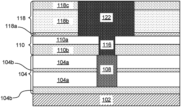
1. A device comprising:
a first oxide layer disposed on a substrate;
a first nitride layer disposed on and interfacing with the first oxide layer;
a second oxide layer disposed on and interfacing with the first nitride layer;
a first conductive feature extending through the first oxide layer, the first nitride layer and the second oxide layer;
a second nitride layer disposed on and interfacing with the second oxide layer;
a third oxide layer disposed on and interfacing with second nitride layer;
a via extending through and interfacing with the second nitride layer and the third oxide layer, wherein the via does not include any barrier layer separating the via from the second nitride layer and the third oxide layer;
a third dielectric layer disposed on and interfacing with the third oxide layer; and
a second conductive feature extending through the third dielectric layer and interfacing with the third dielectric layer and the via, wherein the second conductive feature is formed of the same material as the via, and wherein the second conductive feature does not include any barrier layer separating the second conductive feature from the third dielectric layer.
|
|
8. A device comprising:
a first oxide layer disposed over a substrate;
a first nitride layer disposed over the substrate;
a first conductive feature extending through and interfacing with the first oxide layer and the first nitride layer;
a second oxide layer disposed over the first conductive feature;
a second nitride layer disposed over the first conductive feature;
a via extending through and interfacing with the second oxide layer and the second nitride layer;
a third dielectric layer disposed over the via; and
a second conductive feature extending through the third dielectric layer and interfacing with the third dielectric layer and the via, wherein the second conductive feature is formed of the same material throughout the second conductive feature.
|
|
15. A device comprising:
a first dielectric layer disposed on a substrate, the first dielectric layer having a first thickness;
a first conductive feature disposed within the first dielectric layer;
a second dielectric layer disposed on the first dielectric layer, the second dielectric having a second thickness that is different than the first thickness;
a via disposed within the second dielectric layer and interfacing with the first conductive feature;
a third dielectric layer disposed on the second dielectric layer, the third dielectric layer having a third thickness that is different from the first and second thicknesses; and
a metal layer disposed within the third dielectric layer without a barrier layer being disposed around the metal layer such that the metal layer directly contacts the third dielectric layer and the via, the metal layer being formed of the same material throughout the metal layer.
|