| CPC H01L 21/76802 (2013.01) [H01L 21/0332 (2013.01); H01L 21/0337 (2013.01); H01L 21/31111 (2013.01); H01L 21/31144 (2013.01); H01L 21/76877 (2013.01); H01L 21/823437 (2013.01); H01L 21/823475 (2013.01); H01L 23/5226 (2013.01); H01L 23/5283 (2013.01); H01L 23/53295 (2013.01)] | 20 Claims |
|
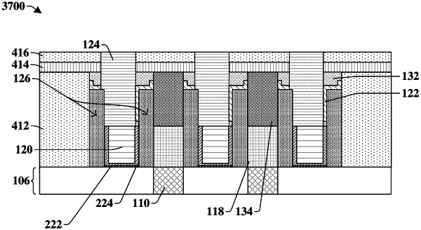
1. An integrated chip structure, comprising:
a substrate;
a gate electrode over the substrate;
a spacer structure laterally surrounding the gate electrode;
a conductive via disposed on the gate electrode;
a liner arranged along one or more sidewalls of the spacer structure; and
wherein the conductive via has a bottommost surface that has a larger width than a part of the conductive via that is laterally adjacent to one or more interior sidewalls of the liner.
|
|
9. An integrated chip structure, comprising:
a substrate;
a gate electrode over the substrate;
a spacer structure surrounding the gate electrode;
a contact via disposed on the gate electrode; and
a liner arranged on one or more sidewalls of the spacer structure, wherein the contact via continuously extends from directly above an upper surface of the liner to directly below a bottom of the liner.
|
|
17. An integrated chip structure, comprising:
a spacer structure extending along a sidewall of a dielectric structure along an interface extending in a first direction in a plan view;
a hard mask structure separated from the dielectric structure by the spacer structure along a second direction, the first direction being perpendicular to the second direction in the plan view;
a contact via surrounded on opposing sides by the hard mask structure along the first direction; and
a liner comprising a first outer sidewall extending along the first direction along a sidewall of the spacer structure and further comprising a second outer sidewall extending along the first direction along sidewalls of both the hard mask structure and the contact via.
|