| CPC H01L 21/6838 (2013.01) [H01L 21/56 (2013.01); H01L 21/6836 (2013.01); H01L 21/68721 (2013.01); H01L 24/03 (2013.01); H01L 2224/0231 (2013.01); H01L 2224/02379 (2013.01)] | 20 Claims |
|
1. A method of manufacturing a semiconductor package, comprising:
providing a semiconductor device on a substrate;
providing an encapsulating material over the substrate to at least laterally encapsulate the semiconductor device and form a reconstructed wafer attaching the reconstructed wafer to a tape carrier;
debonding the substrate from the reconstructed wafer;
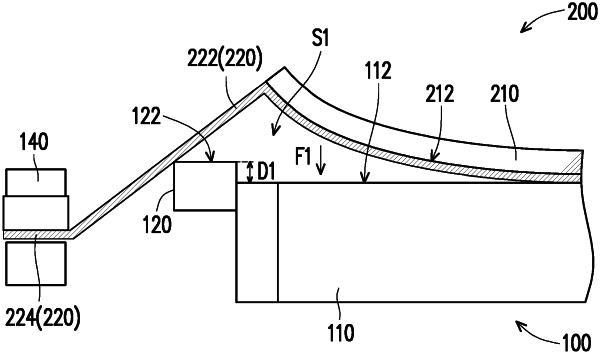
providing the reconstructed wafer with the tape carrier on a wafer chuck, wherein the wafer chuck comprises a chuck body and a seal ring surrounding a periphery of the chuck body, and a top surface of the seal ring is higher than a receiving surface of the chuck body;
fixing the tape carrier outside the chuck body, wherein the tape carrier leans against the seal ring and an enclosed space is formed between the chuck body, the tape carrier and the seal ring;
forming a vacuum seal by evacuating gas from the enclosed space to pull the periphery of the reconstructed wafer toward the chuck body; and
processing the reconstructed wafer on the wafer chuck;
wherein, when the enclosed space is formed between the chuck body, the tape carrier and the seal ring, a vertical distance from an outer edge of the reconstructed wafer to the receiving surface of the chuck body is 1.5 to 5 times as long as a vertical distance from an outer edge of the receiving surface of the chuck body to the tape carrier.
|