| CPC H01L 21/477 (2013.01) [H01L 21/475 (2013.01); H01L 21/47573 (2013.01); H01L 27/0886 (2013.01); H01L 29/42392 (2013.01); H01L 29/517 (2013.01)] | 20 Claims |
|
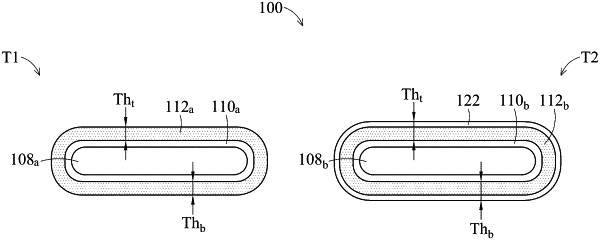
1. An integrated circuit, comprising:
a first transistor having a first threshold voltage and including:
a plurality of stacked first channel regions; and
a first high-K dielectric layer surrounding each of the first channel regions; and
a first gate metal in contact with the first high-K dielectric layer;
a second transistor having a second threshold voltage different than the first threshold voltage and including:
a plurality of stacked second channel regions;
a second high-K dielectric layer surrounding each of the second channel regions;
a first intermixing layer surrounding and in contact with the second high-K dielectric layer; and
a second gate metal in contact with the first intermixing layer, wherein the first intermixing layer includes material from the second high-K dielectric layer and a previously removed first hard mask layer.
|