| CPC H01L 21/3221 (2013.01) [H01L 21/28176 (2013.01); H01L 21/28185 (2013.01); H01L 21/28202 (2013.01); H01L 21/76224 (2013.01); H01L 29/165 (2013.01); H01L 29/66795 (2013.01); H01L 29/7848 (2013.01); H01L 29/7851 (2013.01)] | 20 Claims |
|
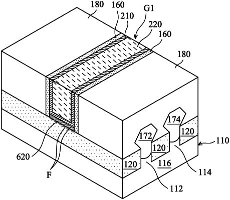
1. A semiconductor device structure, comprising:
a substrate having a base portion and a fin portion over the base portion;
an isolation layer over the base portion and surrounding the fin portion; and
a metal gate stack over the isolation layer and wrapping around an upper part of the fin portion, wherein the metal gate stack comprises a gate dielectric layer and a metal gate electrode layer over the gate dielectric layer, the gate dielectric layer comprises fluorine,
a first part of the isolation layer is not covered by the metal gate stack, the first part comprises fluorine, and a first concentration of fluorine in the first part increases toward a first top surface of the first part.
|