| CPC H01L 21/32139 (2013.01) [H01L 21/02164 (2013.01); H01L 21/02274 (2013.01); H01L 21/0228 (2013.01); H01L 21/31116 (2013.01); H01L 21/31144 (2013.01)] | 20 Claims |
|
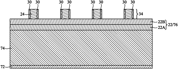
1. A method comprising:
forming a photoresist with a first width over a target layer by a photolithography process;
performing a plasma-enhanced deposition process, the plasma-enhanced deposition process decreasing roughness of sidewalls of the photoresist while depositing a spacer layer, horizontal portions of the spacer layer being deposited on top surfaces of the photoresist, vertical portions of the spacer layer being deposited on the sidewalls of the photoresist, wherein the photoresist has the first width at the start of the plasma-enhanced deposition process, wherein the photoresist has a second width at the end of the plasma-enhanced deposition process;
patterning the spacer layer to form spacers on the sidewalls of the photoresist, wherein patterning the spacer layer comprises performing an etching process, wherein the etching process selectively etches the horizontal portions of the spacer layer at a faster rate than the vertical portions of the spacer layer, wherein the photoresist has the second width at the start of the etching process, wherein the second width is in a range of 15 nm to 80 nm; and
etching the target layer using the spacers and the photoresist as a combined etching mask.
|