| CPC H01L 21/31116 (2013.01) [H01L 21/0274 (2013.01); H01L 21/31144 (2013.01); H01L 21/76816 (2013.01); H01L 21/76877 (2013.01)] | 20 Claims |
|
1. A method of forming patterns, the method comprising:
forming an initial pattern including a plurality of opening patterns in a first layer disposed over a substrate;
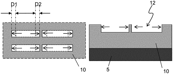
extending the plurality of opening patterns in a first axis by directional etching to form a plurality of exposed groove patterns in plan view,
wherein in the directional etching, an etching rate of the first layer along the first axis is greater than an etching rate of the first layer along a second axis perpendicular to the first axis, the second axis being horizontal and parallel to the surface of the substrate.
|
|
9. A method of forming a pattern, the method comprising:
forming a first conductive pattern embedded in a first dielectric layer disposed over a substrate;
forming a first opening and a second opening in the first dielectric layer;
extending the first and second openings in a first axis by directional etching to form a groove pattern;
forming a second conductive pattern by filling the groove pattern with a conductive material,
wherein in the directional etching, an etching rate of the first dielectric layer along the first axis is greater than an etching rate of the first dielectric layer along a second axis perpendicular to the first axis, the second axis being horizontal and parallel to the surface of the substrate.
|
|
13. A method of manufacturing a semiconductor device, the method comprising:
forming a resist pattern having a plurality of opening patterns over an underlying layer disposed over a substrate;
forming a plurality of openings by etching the underlying layer through the plurality of opening patterns;
extending the plurality of openings in a first axis by directional etching to form a plurality of exposed groove patterns in plan view,
wherein in the directional etching, an etching rate of the underlying layer along the first axis is greater than an etching rate of the underlying layer along a second axis perpendicular to the first axis, the second axis being horizontal and parallel to the surface of the substrate.
|