| CPC H01L 21/31116 (2013.01) [C09K 13/06 (2013.01); H01L 21/02164 (2013.01); H01L 21/823871 (2013.01); H01L 29/401 (2013.01); H01L 21/76897 (2013.01); H01L 29/41733 (2013.01); H01L 29/41783 (2013.01); H01L 29/42392 (2013.01)] | 20 Claims |

|
1. A method for manufacturing a semiconductor device comprising:
forming a feature in a dielectric layer disposed on a semiconductor substrate, the dielectric layer including silicon oxide, the feature extending downwardly from a top surface of the dielectric layer and including silicon, a nitride compound, a low-k dielectric material other than silicon oxide, or combinations thereof; and
selectively etching the dielectric layer using an etchant composition to form a trench extending downwardly from the top surface of the dielectric layer, the etchant composition including a hydrogen halide and a nitrogen-containing compound represented by Formula (A),
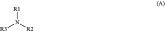 wherein
R1, R2, R3 are each independently hydrogen, methyl, or ethyl, and
wherein the method further comprises, prior to selectively etching the dielectric layer, forming a spacer layer having a wall portion which extends downwardly from the top surface of the dielectric layer and which is disposed between the dielectric layer and the feature, the spacer layer including a nitride compound, a low-k dielectric material other than silicon oxide, or a combination thereof.
|