| CPC H01L 21/3086 (2013.01) [C23C 16/26 (2013.01); H01L 21/02274 (2013.01); H01L 21/0335 (2013.01); H01L 21/0337 (2013.01); H01L 23/298 (2013.01)] | 20 Claims |
|
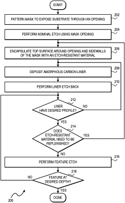
1. A method for fabricating a feature into a semiconductor substrate, the method comprising:
(a) encapsulating with an etch-resistant material around an opening and sidewalls of a mask defining the feature nominally etched into the semiconductor substrate;
(b) depositing an amorphous carbon liner on the sidewalls of the mask and sidewalls of the feature;
(c) performing an amorphous carbon liner etch for removing excess amorphous carbon deposited around the opening or the sidewalls of the mask during the deposition of the amorphous carbon liner, the etch-resistant material preventing or mitigating etching of the around the opening and the sidewalls of the mask during the amorphous carbon liner etch; and
(d) performing a feature etch to deepen a depth of the feature into the semiconductor substrate.
|