US 12,266,525 B2
Photomask pellicle including network of nanowires and method of forming the same
Yun-Yue Lin, Hsinchu (TW); and Chen-Chieh Yu, Hsinchu (TW)
Assigned to TAIWAN SEMICONDUCTOR MANUFACTURING COMPANY LTD., Hsinchu (TW)
Filed by TAIWAN SEMICONDUCTOR MANUFACTURING COMPANY LTD., Hsinchu (TW)
Filed on Jan. 30, 2024, as Appl. No. 18/426,387.
Application 18/426,387 is a continuation of application No. 17/351,219, filed on Jun. 17, 2021, granted, now 11,923,196.
Claims priority of provisional application 63/156,734, filed on Mar. 4, 2021.
Prior Publication US 2024/0177994 A1, May 30, 2024
This patent is subject to a terminal disclaimer.
Int. Cl. H01L 21/02 (2006.01); G03F 1/64 (2012.01); H01L 21/033 (2006.01); H01L 29/06 (2006.01)
CPC H01L 21/02603 (2013.01) [G03F 1/64 (2013.01); H01L 21/02444 (2013.01); H01L 21/0332 (2013.01); H01L 21/0337 (2013.01); H01L 29/0669 (2013.01)] 20 Claims
OG exemplary drawing
 
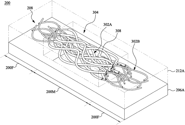
13. A method, comprising:
depositing a first capping layer over a substrate;
growing a network of nanowires over the first capping layer;
depositing a second capping layer over the network of nanowires, wherein the first capping layer and the second capping layer encapsulate the nanowires; and
etching the first capping layer and the second capping layer to form a coating, from the first capping layer and the second capping layer, on a first portion of the nanowires, wherein a plurality of gaps is formed between the nanowires.