| CPC H01G 4/224 (2013.01) [H01G 4/232 (2013.01); H01G 4/248 (2013.01); H01G 4/30 (2013.01)] | 28 Claims |
|
1. A multilayer ceramic electronic component comprising:
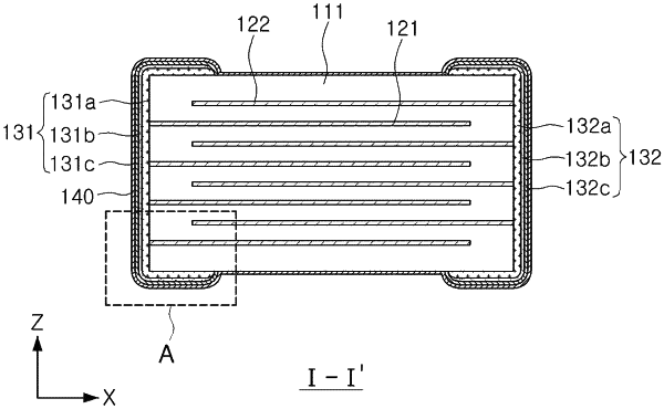
a ceramic body including dielectric layers and first internal electrodes and second internal electrodes disposed to face each other and alternately stacked with the respective dielectric layers interposed therebetween;
a first external electrode connected to the first internal electrodes;
a second external electrode connected to the second internal electrodes; and
a protective layer disposed on the ceramic body, the first external electrode, and the second external electrode,
wherein the protective layer includes an adhesion assisting layer and a coating layer,
an average thickness of the protective layer is 70 nm or more and less than 400 nm, and
a ratio of an average thickness of the coating layer to the average thickness of the protective layer is 0.25 or more and 0.75 or less.
|