| CPC G11C 29/46 (2013.01) [G11C 29/12005 (2013.01); G11C 29/36 (2013.01); G11C 2029/3602 (2013.01)] | 20 Claims |
|
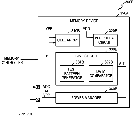
1. A memory device comprising:
a cell array comprising a plurality of memory cells;
a peripheral circuit configured to control a memory operation of the plurality of memory cells;
a test logic circuit configured to operate in a test mode and configured to perform a test operation on the plurality of memory cells;
a first regulator configured to regulate a first power supply voltage received through a first pad and provide the first power supply voltage to at least one of the cell array and the peripheral circuit; and
a power manager between the first pad and an input terminal of the first regulator, and between the first pad and the test logic circuit,
wherein the power manager is configured to provide a test power supply voltage generated through a power processing operation for the first power supply voltage to the test logic circuit,
wherein, in the test mode, while a first target voltage level of the first regulator fluctuates, a second target voltage level of the power manager is maintained constant.
|