| CPC G09G 3/3291 (2013.01) [G09G 3/3233 (2013.01); G09G 2300/0819 (2013.01); G09G 2300/0852 (2013.01); G09G 2310/0251 (2013.01)] | 9 Claims |
|
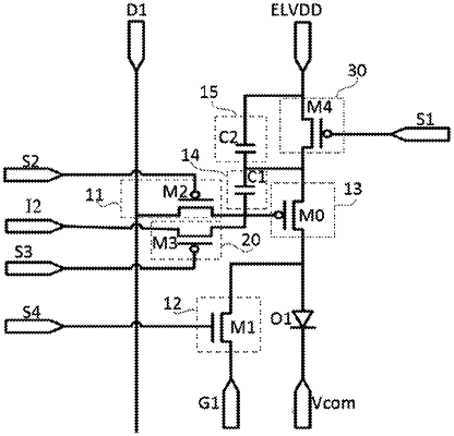
1. A pixel circuit, comprising a light-emitting element, a data writing circuit, a first control circuit, a driving circuit, a first power storage circuit, and a second power storage circuit, wherein:
the first control circuit is electrically connected to a first control terminal, a first electrode of the light-emitting element and a first initial voltage terminal, and is configured to write a first initial voltage provided by the first initial voltage terminal into the first electrode of the light-emitting element under control of a first control signal provided by the first control terminal in a non-light-emitting phase;
a first terminal of the first power storage circuit is electrically connected to a control terminal of the driving circuit, a second terminal of the first power storage circuit is electrically connected to a first terminal of the driving circuit, and the first power storage circuit is configured to store electric energy;
a first terminal of the second power storage circuit is electrically connected to the first terminal of the driving circuit, a second terminal of the second power storage circuit is electrically connected to a first voltage terminal, and the second power storage circuit is configured to store electric energy;
the data writing circuit is electrically connected to a writing control terminal, a data line and the control terminal of the driving circuit, and is configured to write a data voltage provided by the data line into the control terminal of the driving circuit under control of a writing control signal provided by the writing control terminal;
a second terminal of the driving circuit is electrically connected to the first electrode of the light-emitting element, and the driving circuit is configured to drive the light-emitting element to emit light under control of a potential of the control terminal of the driving circuit; a second electrode of the light-emitting element is electrically connected to a second voltage terminal;
the pixel circuit further comprises a reset circuit, the reset circuit is electrically connected to a reset control terminal, a second initial voltage terminal, and the control terminal of the driving circuit, and the reset circuit is configured to write a second initial voltage provided by the second initial voltage terminal into the control terminal of the driving circuit under control of a reset control signal provided by the reset control terminal;
the pixel circuit further comprises a light-emitting control circuit, the light-emitting control circuit is electrically connected to a light-emitting control terminal, the first voltage terminal, and the first terminal of the driving circuit, and the light-emitting control circuit is configured to control the first voltage terminal to be connected to the first terminal of the driving circuit under control of a light-emitting control signal provided by the light-emitting control terminal;
the first control circuit comprises a first transistor, a control electrode of the first transistor is electrically connected to the first control terminal, a first electrode of the first transistor is electrically connected to the first initial voltage terminal, and a second electrode of the first transistor is electrically connected to the first electrode of the light-emitting element;
the light-emitting control circuit comprises a fourth transistor, a control electrode of the fourth transistor is electrically connected to the light-emitting control terminal, a first electrode of the fourth transistor is electrically connected to the first voltage terminal, and a second electrode of the fourth transistor is electrically connected to the first terminal of the driving circuit;
the first transistor is an n-type transistor, the fourth transistor is a p-type transistor, the first control terminal is configured to provide a first control signal, and the light-emitting control terminal is configured to provide a light-emitting control signal; and
in a display cycle, a time period for which a potential of a first control signal connected to the control electrode of the first transistor is maintained at a high voltage is longer than a time period for which a potential of a light-emitting control signal connected to the control electrode of the fourth transistor is maintained at the high voltage.
|