| CPC G09G 3/3291 (2013.01) [G09G 2310/027 (2013.01); G09G 2320/0276 (2013.01); G09G 2330/021 (2013.01)] | 15 Claims |

|
1. A data driving circuit, comprising:
a plurality of data input terminals to which pixel data of an input image is input;
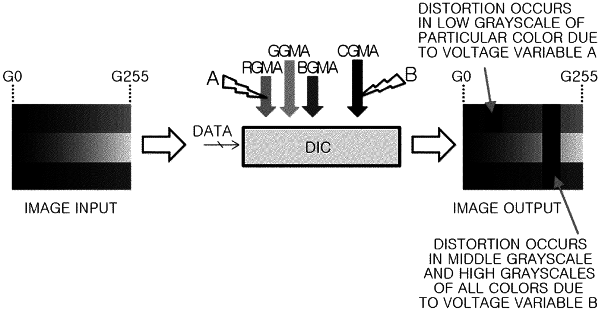
a plurality of voltage input terminals to which gamma tab voltages for each color having different voltage levels, and common gamma tab voltages having different voltage levels are each input; and
a plurality of output terminals to which a data voltage of a first color, a data voltage of a second color, and a data voltage of a third color are output,
wherein:
a data voltage range of the first color includes a low grayscale voltage range of the first color obtained from the gamma tab voltages of the first color, and a middle grayscale and high grayscale voltage range of the first color obtained from the common gamma tab voltages,
a data voltage range of the second color includes a low grayscale voltage range of the second color obtained from the gamma tab voltages of the second color, and a middle grayscale and high grayscale voltage range of the second color obtained from the common gamma tab voltages,
a data voltage range of the third color includes a low grayscale voltage range of the third color obtained from the gamma tab voltages of the third color, and a middle grayscale and high grayscale voltage range of the third color obtained from the common gamma tab voltages,
a minimum voltage of a common middle grayscale and high grayscale voltage range obtained from the common gamma tab voltages is configured to be set to a smallest minimum voltage among minimum voltages of data voltage ranges of the first color, the second color, and the third color, and
a maximum voltage of the common middle grayscale and high grayscale voltage range is configured to be set to a maximum voltage among reference grayscale voltages of the data voltage ranges of the first color, the second color, and the third color.
|