| CPC G09G 3/3233 (2013.01) [G09G 2300/0426 (2013.01); G09G 2300/0819 (2013.01); G09G 2300/0842 (2013.01); G09G 2310/08 (2013.01); G09G 2320/0233 (2013.01); G09G 2320/0247 (2013.01)] | 20 Claims |
|
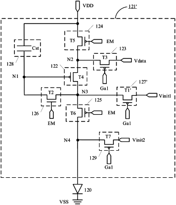
1. A pixel circuit, comprising a driving sub-circuit, a data writing sub-circuit, a first light-emitting control sub-circuit, a second light-emitting control sub-circuit, a compensation sub-circuit, a first reset sub-circuit, and a second reset sub-circuit, and configured to generate a driving current to control a light-emitting element to emit light,
wherein the driving sub-circuit comprises a control terminal, a first terminal, and a second terminal;
the data writing sub-circuit is electrically connected to the first terminal of the driving sub-circuit and a data signal terminal, and is configured to write a data signal of the data signal terminal into the first terminal of the driving sub-circuit in response to a signal of a first scan signal terminal;
the compensation sub-circuit is electrically connected to the second terminal of the driving sub-circuit and the control terminal of the driving sub-circuit, and is configured to perform threshold compensation on the driving sub-circuit in response to a signal of a compensation control signal terminal;
the first reset sub-circuit is electrically connected to a second voltage terminal, and is configured to write a signal of the second voltage terminal into the control terminal of the driving sub-circuit in response to a signal of a second scan signal terminal;
the second reset sub-circuit is electrically connected to a first electrode of the light-emitting element and a third voltage terminal, and is configured to write a signal of the third voltage terminal into the first electrode of the light-emitting element in response to a signal of a reset control signal terminal to reset the first electrode of the light-emitting element,
wherein the compensation sub-circuit comprises a second transistor, the data writing sub-circuit comprises a third transistor, the second transistor is an oxide transistor, and an active layer type of the second transistor is different from an active layer type of a transistor comprised in at least one selected from a group consisting of the driving sub-circuit, the data writing sub-circuit, the first light-emitting control sub-circuit, and the second light-emitting control sub-circuit; and
a duration when the signal of the second scan signal terminal is in an active state for one time is greater than a duration when the third transistor is turned on for one time.
|