| CPC G09G 3/3233 (2013.01) [H10K 59/1315 (2023.02); G09G 2300/0408 (2013.01); G09G 2300/0426 (2013.01); G09G 2300/0452 (2013.01); G09G 2300/0819 (2013.01); G09G 2300/0842 (2013.01); G09G 2300/0861 (2013.01); G09G 2310/0272 (2013.01); G09G 2310/08 (2013.01); G09G 2320/043 (2013.01); G09G 2330/026 (2013.01)] | 17 Claims |
|
1. A display substrate, comprising:
a base substrate; and
a plurality of sub-pixels, arranged in a plurality of pixel rows along a first direction and a plurality of pixel columns along a second direction on the base substrate,
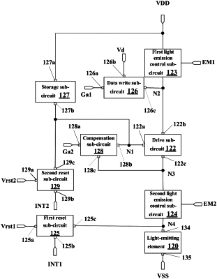
wherein each of the plurality of sub-pixels comprises a pixel circuit, and the pixel circuit is configured to drive a light-emitting element corresponding to the each sub-pixel to emit light;
the pixel circuit comprises a drive sub-circuit and a first reset sub-circuit;
the drive sub-circuit comprises a control terminal, a first terminal, and a second terminal, and the drive sub-circuit is configured to be connected with the light-emitting element and control a drive current flowing through the light-emitting element;
the first reset sub-circuit comprises a control terminal, a first terminal and a second terminal, the control terminal of the first reset sub-circuit is configured to receive a first reset control voltage, the first terminal of the first reset sub-circuit is configured to receive a first reset voltage, and the second terminal of the first reset sub-circuit is connected with the control terminal of the drive sub-circuit; the first rest sub-circuit is configured to apply the first reset voltage to the control terminal of the drive sub-circuit in response to the first reset control voltage;
the display substrate further comprises a first reset signal line extended along the first direction, the first reset signal line is electrically connected with the first terminal of the first reset sub-circuit to provide the first reset voltage, and the first reset signal line is in a semiconductor layer and comprises a doped semiconductor material;
the pixel circuit further comprises a second reset sub-circuit, and the second reset sub-circuit comprises a control terminal, a first terminal and a second terminal, the control terminal of the second reset sub-circuit is configured to receive a second reset control voltage, the first terminal of the second reset sub-circuit is configured to receive a second reset voltage, and the second terminal of the second reset sub-circuit is configured to be connected with the light emitting element;
the pixel circuit further comprises a light emission control sub-circuit;
the light emission control sub-circuit comprises a control terminal, a first terminal and a second terminal, the first terminal of the light emission control sub-circuit is connected with the second terminal of the drive sub-circuit, and the second terminal of the light emission control sub-circuit is configured to be connected with the light-emitting element;
the second reset sub-circuit comprises a reset transistor comprising a gate electrode, a first electrode and a second electrode which respectively serve as the control terminal, the first terminal and the second terminal of the second reset sub-circuit, and the light emission control sub-circuit comprises a light emission control transistor comprising a gate electrode, a first electrode and a second electrode which respectively serve as the control terminal, the first terminal and the second terminal of the light emission control sub-circuit;
the second electrode of the reset transistor and the second electrode of the light emission control transistor are both in the semiconductor layer and are spaced apart from each other, and are electrically connected with each other by a first connection electrode; and
the first connection electrode is on a side of the semiconductor layer away from the base substrate.
|