| CPC G09G 3/3233 (2013.01) [G09G 2300/0426 (2013.01); G09G 2300/0465 (2013.01); G09G 2300/0842 (2013.01)] | 20 Claims |
|
1. A display device, comprising a base substrate, at least one pixel circuit, and a light-emitting element,
wherein the pixel circuit and the light-emitting element are on the base substrate;
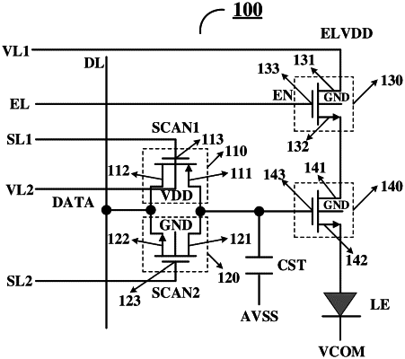
the pixel circuit comprises a driving transistor, the driving transistor comprises a control electrode, a first electrode, and a second electrode, and the driving transistor is configured to control a driving current, flowing through the first electrode of the driving transistor and the second electrode of the driving transistor, for driving the light-emitting element to emit light according to a voltage of the control electrode of the driving transistor; and
the pixel circuit further comprises a first transistor, a first electrode of the first transistor is electrically connected to the control electrode of the driving transistor through a first transfer electrode and a second transfer electrode, and an extending direction of the second transfer electrode is perpendicular to an extending direction of the first transfer electrode.
|