| CPC G02F 1/025 (2013.01) [H01S 5/0601 (2013.01); G02F 1/0157 (2021.01); G02F 2202/101 (2013.01); G02F 2202/102 (2013.01); G02F 2202/108 (2013.01)] | 8 Claims |
|
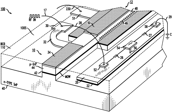
1. An electro-absorption optical modulator, comprising:
a substrate;
an electro-absorption modulating (EAM) device formed on the substrate, the EAM device having an optical input for receiving a continuous wave (CW) optical signal, an optical output for emitting a modulated optical output signal;
an RF input signal path coupled to the EAM device for providing a modulated electrical input signal to the EAM device;
an on-chip AC ground plane disposed on the substrate; and
a resistive RF signal termination path coupled between the on-chip AC ground plane and the RF input signal path, the on-chip AC ground plane terminating a high frequency portion of the modulated electrical input signal.
|