| CPC G01R 31/318597 (2013.01) [G01R 31/31908 (2013.01)] | 9 Claims |
|
1. A universal test chiplet, wherein the universal test chiplet is configured to test M chiplets to be tested, M is a positive integer, and the universal test chiplet comprising:
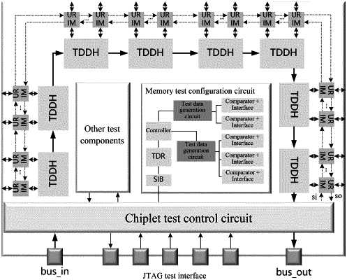
a chiplet test control circuit, wherein the chiplet test control circuit is connected to the chiplets to be tested, a test data distribution circuit, a memory test configuration circuit and a chiplet test interface circuit, wherein the chiplet test control circuit is configured to receive external JTAG signals and to configure JTAG signals of the chiplets to be tested, as well as to provide test data and configure test modes for the chiplets to be tested, and to provide configuration signals for the memory test configuration circuit, the chiplet test interface circuit, and the chiplets to be tested;
the test data distribution circuit, which is connected to the chiplet test control circuit and the chiplet test interface circuit, wherein the test data distribution circuit comprises N test data channels, wherein N is a positive integer, and the test data distribution circuit is configured to distribute test data required by each of the chiplets to be tested from a test data bus, so as to load or unload the test data channels;
the memory test configuration circuit, which is connected to a memory of the chiplets to be tested and the chiplet test control circuit, wherein the memory test configuration circuit is configured to provide test circuits for the memory of the chiplets to be tested and automatically generate a test vector; and
the chiplet test interface circuit, which is connected to the chiplets to be tested, the chiplet test control circuit, and the test data distribution circuit, wherein the chiplet test interface circuit is configured to connect the test data channels into a single chain, and to transmit the test data to the chiplets to be tested, along any direction including up, down, left, right, through chiplet test interfaces,
wherein the chiplet test control circuit comprises a test state control circuit unit, a test instruction circuit unit, a test sub-interface control circuit unit, and a test data circuit unit; wherein
the test state control circuit unit comprises a finite-state machine, and is configured to enable register enable signals activated in different test cycles, and transmit the register enable signals to the test sub-interface control circuit unit and the test instruction circuit unit;
the test instruction circuit unit comprises a multi-bit instruction register, and each type of test code corresponds to one test instruction; and the test instruction circuit unit is configured to receive the register enable signals from the test state control circuit unit, generate corresponding test instruction enable signals, and transmit the test instruction enable signals to a test data circuit;
the test sub-interface control circuit unit is configured to receive external JTAG signals and configure the JTAG signals of the chiplets to be tested, output test responses to an external system, and string test data chains into a single chain; and
the test data circuit unit comprises a plurality of registers to provide configuration signals for the corresponding test sub-interface control circuit unit, the memory test configuration circuit and the chiplet test interface circuit according to the test instruction enable signals, and the test data circuit unit further comprises an IJTAG network to provide configuration signals for the test data distribution circuit.
|