| CPC G01R 31/2896 (2013.01) [G01R 1/0441 (2013.01); H01L 23/5226 (2013.01); H01L 24/16 (2013.01); H01L 24/32 (2013.01); H01L 24/73 (2013.01); H01L 2224/16225 (2013.01); H01L 2224/32225 (2013.01); H01L 2224/73204 (2013.01)] | 20 Claims |
|
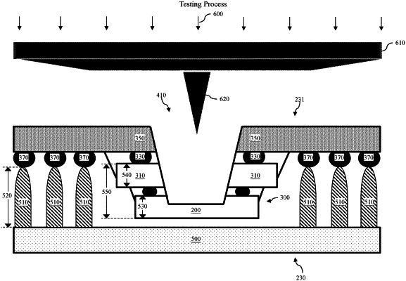
1. An apparatus, comprising:
a socket of a testing tool configured to provide testing signals;
a device-under-test (DUT) board configured to provide electrical routing; and
an integrated circuit (IC) die disposed between the socket and the DUT board, wherein the testing signals are electrically routed to the IC die through the DUT board, and wherein the IC die includes a substrate in which plurality of transistors is formed, a first structure that contains a plurality of first metallization components, and a second structure that contains a plurality of second metallization components, wherein the first structure is disposed over a first side of the substrate, and wherein the second structure is disposed over a second side of the substrate opposite the first side.
|