| CPC G01J 5/20 (2013.01) [H10N 19/00 (2023.02)] | 24 Claims |
|
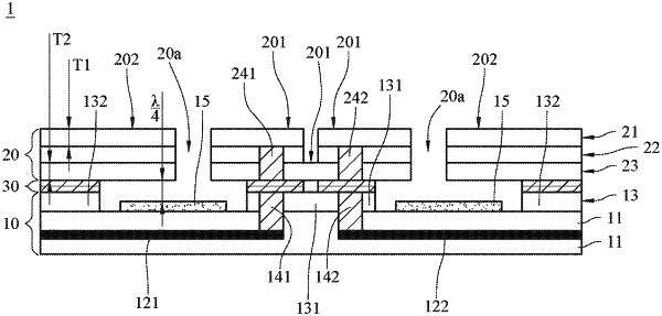
1. A vertically integrated micro-bolometer, for sensing an infrared ray with a wavelength, comprising:
an integrated circuit chip comprising:
a silicon substrate;
a circuit element; and
a dielectric layer disposed on the silicon substrate and exposing a part of the silicon substrate;
an infrared sensing film being a flat multilayer structure, comprising:
a top absorbing layer;
a bottom absorbing layer, wherein materials of the top absorbing layer and the bottom absorbing layer are materials compatible with a semiconductor manufacturing process; and
a sensing layer disposed between the top absorbing layer and the bottom absorbing layer, wherein a material of the sensing layer is silicon germanium alloy (SiGe) or silicon carbide (SiC) which are materials compatible with a semiconductor manufacturing process; and
a metal bonding layer connecting the dielectric layer and the bottom absorbing layer so that the infrared sensing film is vertically integrated on the integrated circuit chip and the sensing layer is electrically connected to the circuit element.
|