| CPC G01D 5/2053 (2013.01) [G01B 7/30 (2013.01); G01D 5/24438 (2013.01)] | 8 Claims |
|
1. An inductive rotor position sensor device for detecting a rotor angular position of a rotor of an electric machine, the inductive rotor position sensor device comprising:
a transmitter coil configured to generate electromagnetic waves;
a receiver coil configured to detect the electromagnetic waves generated by the transmitter coil and influenced by the rotor;
a processing unit configured to activate the transmitter coil and to evaluate the electromagnetic waves detected by the receiver coil for determining the rotor angular position; and
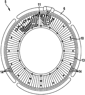
a rigid multi-layer circuit board comprising two outer layers, namely a front side and a rear side which faces away from the front side, and several inner layers, the transmitter and receiver coils and the processing unit being situated on the circuit board, wherein the transmitter and receiver coils are situated on the front side of the circuit board, and the processing unit is situated on the rear side of the circuit board, wherein:
at least one shielding layer for shielding the processing unit against the electromagnetic waves is situated between the coils and the processing unit,
a further shielding layer rests on the at least one shielding layer, each of the further shielding layer and the at least one shielding layer have multiple slots and are configured to be situated on top of one another in such a way that none of the slots overlap, and
the shielding layers are lithographically applied as inner layers to the circuit board and etched out of a copper cladding.
|