| CPC C23C 16/345 (2013.01) [C23C 16/36 (2013.01); C23C 16/45553 (2013.01); C23C 16/52 (2013.01)] | 11 Claims |
|
1. A method for forming a silicon-containing film on the surface of a microelectronic device, which comprises introducing at least one compound of Formula (I):
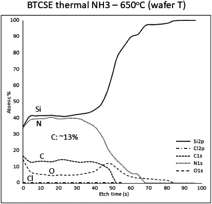
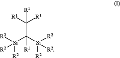 wherein each R1 is independently chosen from hydrogen or C1-C4 alkyl, and each R2 is independently chosen from chloro, bromo, iodo, hydrogen, or C1-C4 alkyl, provided that no fewer than two of R2 is chosen from chloro, bromo, or iodo, to said surface in a reaction chamber, under atomic layer deposition conditions at a temperature of greater than 600° C., the atomic layer deposition conditions are non-plasma conditions, the silicon-containing film is free of halides, the silicon-containing film is a silicon nitride film with about 9% to about 13% carbon with a silicon to nitrogen ratio of about 1:1, and wherein the compound of Formula (I) has a purity of greater than 98%.
|