| CPC H10K 59/353 (2023.02) [H10K 59/1213 (2023.02); H10K 59/1216 (2023.02); H10K 59/122 (2023.02); H10K 59/131 (2023.02)] | 21 Claims |

|
1. A display substrate, the display substrate comprising a display area and a non-display area, wherein the display substrate comprises:
a base substrate;
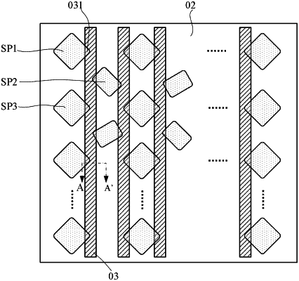
a plurality of sub-pixels in the display area, wherein the plurality of sub-pixels are arranged on the base substrate in an array in a row direction and a column direction, each sub-pixel comprises a light-emission device, and the light-emission device comprises a first electrode;
a plurality of signal lines on the base substrate, wherein the plurality of signal lines comprise at least a first signal line and a second signal line, the first signal line is configured to transmit a voltage signal, and the second signal line is configured to transmit a scan signal;
a signal line lead on the base substrate, wherein the signal line lead is located in the non-display area; and
a signal line transfer structure on the base substrate, wherein the signal line transfer structure is configured to connect the signal line lead and the second signal line,
wherein the signal line transfer structure and the first signal line are located in the same layer, and the signal line transfer structure is spaced apart from the first signal line; and
wherein an orthographic projection of the first electrode of at least one of the sub-pixels on the base substrate at least partially overlaps with an orthographic projection of the first signal line on the base substrate, and the orthographic projection of the first electrode of at least one of the sub-pixels on the base substrate at least partially overlaps with an orthographic projection of the signal line transfer structure on the base substrate.
|