| CPC H03K 3/0372 (2013.01) [H01L 27/105 (2013.01); H01L 29/02 (2013.01); H01L 29/06 (2013.01); H01L 29/1075 (2013.01); H01L 29/41725 (2013.01); H03K 3/288 (2013.01); H03K 3/289 (2013.01); H03K 3/356017 (2013.01); H03K 3/356104 (2013.01); H03K 3/356113 (2013.01); H03K 3/356147 (2013.01); H03K 3/3562 (2013.01); H03K 3/35625 (2013.01)] | 20 Claims |

|
1. A method of forming a semiconductor device, comprising:
forming active regions including doping areas of a substrate;
forming source/drain (S/D) regions including doping first areas of the active regions, the S/D regions representing first transistor-components, wherein second areas of the active regions which are between corresponding S/D regions are channel regions representing second transistor-components;
forming gate lines over corresponding ones of the channel regions, the gate lines representing third transistor-components; and
forming metal-to-S/D (MD) contact structures over corresponding ones of the S/D regions, the MD contact structures representing fourth transistor-components; and
the forming the active regions, the forming the S/D regions, the forming the MD contact structures and the forming the gate lines resulting in:
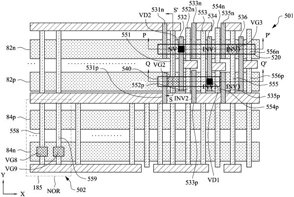
a first set of the first to fourth transistor-components connected as corresponding transistors that define a first time delay circuit having a first input configured to receive a first clock signal and having a first output configured to generate a second clock signal from the first clock signal, wherein the first time delay circuit further includes a first gate line intersecting a first-type active region and a second-type active region in a first area; and
a second set of the first to fourth transistor-components connected as corresponding transistors that define a second time delay circuit having a second input configured to receive the second clock signal and having a second output configured to generate a third clock signal from the first clock signal, wherein the second time delay circuit further includes a second gate line intersecting the first-type active region and the second-type active region in a second area;
forming a first gate via-connector in direct contact with the first gate line atop the first-type active region in the first area; and
forming a second gate via-connector in direct contact with the second gate line atop the second-type active region in the second area.
|