| CPC H01L 33/0093 (2020.05) [H01L 33/0066 (2013.01); H01L 33/30 (2013.01)] | 20 Claims |

|
1. A display device comprising:
a first electrode and a second electrode spaced from each other on a substrate; and
a light-emitting element on the first electrode and the second electrode,
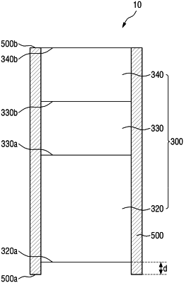
wherein the light-emitting element comprises a first semiconductor layer and a second semiconductor layer, an active layer between the first semiconductor layer and the second semiconductor layer, and an insulating film surrounding at least a portion of the active layer, the first semiconductor layer, the active layer, and the second semiconductor layer being stacked along a height direction of the light-emitting element,
wherein the light-emitting element has an aspect ratio of a height of the light-emitting element to a width of the light-emitting element that is greater than 1,
wherein a first end portion of the insulating film protrudes to extend beyond a first surface of the first semiconductor layer, and
wherein the first surface is an opposite surface of a second surface of the first semiconductor layer facing the active layer.
|