| CPC H01L 31/076 (2013.01) [H01L 31/02363 (2013.01); H01L 31/028 (2013.01); H01L 31/077 (2013.01); H01L 31/1804 (2013.01); H01L 31/186 (2013.01)] | 19 Claims |

|
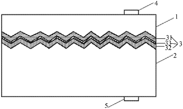
1. A tandem photovoltaic device, comprising an upper cell unit, a lower cell unit and a tunnel junction located between the upper cell unit and the lower cell unit, wherein the lower cell unit is a crystalline silicon cell;
the tunnel junction comprises a carrier transport layer, a crystalline silicon layer and an intermediate layer located between the carrier transport layer and the crystalline silicon layer, wherein the carrier transport layer is a metal oxide layer, and the intermediate layer comprises a tunneling layer;
the carrier transport layer and the crystalline silicon layer are in direct contact with the intermediate layer, respectively, and a doping concentration of the crystalline silicon layer is greater than or equal to 1017 cm−3;
the carrier transport layer is in direct contact with a shadow surface of the upper cell unit;
when the crystalline silicon layer is a p-type crystalline silicon layer, a first energy level E1 and a second energy level E2 satisfy E1−E2≤0.5 eV, wherein the first energy level E1 is an energy level at a bottom of a conduction band of a metal oxide at an interface where the metal oxide layer contacts the intermediate layer, and the second energy level E2 is an energy level at a top of a valence band of a p-type crystalline silicon at an interface where the intermediate layer contacts the p-type crystalline silicon layer; and
when the crystalline silicon layer is an n-type crystalline silicon layer, a third energy level E3 and a fourth energy level E4 satisfy −0.5 eV≤E3−E4≤0.5 eV, wherein the third energy level E3 is an energy level at a top of a valence band of the metal oxide at the interface where the metal oxide layer contacts the intermediate layer, and the fourth energy level E4 is an energy level at a bottom of a conduction band of an n-type crystalline silicon at an interface where the intermediate layer contacts the n-type crystalline silicon layer.
|