| CPC H01L 29/78696 (2013.01) [H01L 21/823412 (2013.01); H01L 21/823418 (2013.01); H01L 21/823437 (2013.01); H01L 27/088 (2013.01); H01L 29/0673 (2013.01); H01L 29/1608 (2013.01); H01L 29/161 (2013.01); H01L 29/165 (2013.01); H01L 29/42392 (2013.01); H01L 29/66545 (2013.01); H01L 29/7848 (2013.01); H01L 29/78618 (2013.01); H10B 10/12 (2023.02); H10B 10/18 (2023.02)] | 20 Claims |

|
1. A method of forming a semiconductor device, the method comprising:
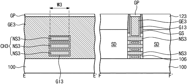
forming sacrificial layers and first semiconductor layers alternately and repeatedly on a transistor region on a substrate including first, second, and third transistor regions;
patterning the sacrificial layers and the first semiconductor layers to form first, second and third preliminary channel regions on the first, second, and third transistor regions respectively, the first, second and third preliminary channel regions having widths different from each other and each including first semiconductor patterns and preliminary sacrificial patterns;
forming dummy gates on the first, second and third preliminary channel regions;
patterning the first, second and third preliminary channel regions to forma first channel portion, second channel portions, third channel portions and sacrificial patterns;
forming source and drain regions on opposite sidewalls of the dummy gates;
removing the dummy gates and the sacrificial patterns to form first, second, and third trenches on the first, second, and third transistor regions;
forming a gate insulation layer and a gate electrode in each of the first, second, third trenches,
wherein the first channel portion is connected to the substrate and has a shape of a fin protruding from an upper surface of the substrate,
wherein the second channel portions are spaced apart from each other in a first direction, perpendicular to the upper surface of the substrate, and
wherein the third channel portions are spaced apart from each other in the first direction.
|