| CPC H01L 29/78618 (2013.01) [H01L 29/0665 (2013.01); H01L 29/42392 (2013.01); H01L 29/78696 (2013.01)] | 20 Claims |

|
1. A semiconductor device comprising:
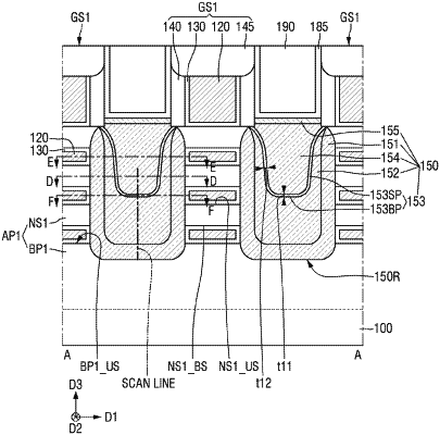
a multi-channel active pattern;
a plurality of gate structures on the multi-channel active pattern and spaced apart from each other in a first direction, the plurality of gate structures including a gate electrode extending in a second direction different from the first direction;
a source/drain recess between an adjacent pair of the plurality of gate structures; and
a source/drain pattern on the multi-channel active pattern in the source/drain recess,
wherein the source/drain pattern includes:
a semiconductor liner layer including silicon-germanium and extending along the source/drain recess,
a semiconductor filling layer including silicon-germanium on the semiconductor liner layer, and
at least one or more semiconductor insertion layers between the semiconductor liner layer and the semiconductor filling layer, and
wherein the at least one or more semiconductor insertion layers have a three-dimensional saddle structure including a saddle point, a first saddle region on opposite sides of the saddle point in the second direction, and a second saddle region on opposite sides of the saddle point in the first direction.
|