| CPC H01L 27/1225 (2013.01) [G06F 1/26 (2013.01); H01L 27/1237 (2013.01); H01L 27/1248 (2013.01); H01L 27/1251 (2013.01); H02J 13/00 (2013.01); H02J 13/00016 (2020.01); H04L 41/069 (2013.01); H04L 47/2416 (2013.01); H04L 67/12 (2013.01); H01L 29/42384 (2013.01); H01L 2029/42388 (2013.01); H01L 29/513 (2013.01); H01L 29/517 (2013.01); H01L 29/518 (2013.01); H01L 29/78606 (2013.01); H01L 29/78633 (2013.01); H01L 29/78675 (2013.01); H01L 29/7869 (2013.01); H04Q 9/02 (2013.01); H04Q 2209/826 (2013.01)] | 5 Claims |
|
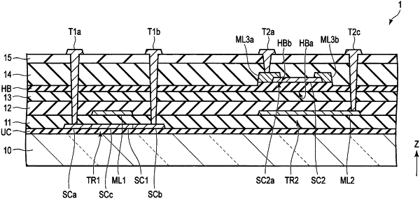
1. An electronic device comprising:
a substrate;
a silicon nitride film formed on the substrate;
a first silicon oxide film formed on the silicon nitride film;
a block insulating layer including oxide on the first silicon oxide film;
a metal oxide semiconductor layer formed on the block insulating layer;
a second silicon oxide film covering the metal oxide semiconductor layer;
a gate electrode formed between the substrate and the silicon nitride film, and facing the metal oxide semiconductor layer, and
a terminal that passes through the silicon nitride film, the first silicon oxide film, and the block insulating layer and that is electrically connected to the gate electrode, wherein
a thickness of the second silicon oxide film is larger than a thickness of the first silicon oxide film,
the thickness of the second silicon oxide film is larger than a thickness of the silicon nitride film,
a first thickness of the block insulating layer is a thickness of a position overlapping the metal oxide semiconductor layer,
a second thickness of the block insulating layer is a thickness of a position not overlapping the metal oxide semiconductor layer, and
the first thickness is larger than the second thickness.
|