| CPC H01L 27/016 (2013.01) [H01L 21/707 (2013.01); H01L 28/60 (2013.01)] | 20 Claims |

|
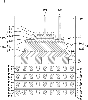
1. A semiconductor structure, comprising:
a first metal-dielectric-metal layer, comprising:
a plurality of first fingers electrically connected to a first voltage;
a plurality of second fingers electrically connected to a second voltage different from the first voltage, wherein the first fingers and the second fingers are arranged in parallel and staggeredly; and
a first dielectric material between the first fingers and the second fingers;
a first dielectric layer over the first metal-dielectric-metal layer;
a first conductive layer over the first dielectric layer;
a second conductive layer over the first conductive layer; and
a second dielectric layer between the first conductive layer and the second conductive layer;
wherein one of the first fingers is connected to a first terminal which electrically connects to an anode of a diode, and the diode includes at least one of a laser diode, a CMOS image sensor (CIS) pixel unit, an OLED pixel unit, or a combination thereof; and
wherein the second conductive layer or one of the second fingers is connected to a second terminal which is configured to receive a first voltage lower than a voltage at the first terminal.
|