| CPC H01L 25/50 (2013.01) [H01L 21/4853 (2013.01); H01L 21/4857 (2013.01); H01L 21/486 (2013.01); H01L 21/568 (2013.01); H01L 21/6835 (2013.01); H01L 23/3128 (2013.01); H01L 23/5384 (2013.01); H01L 23/5389 (2013.01); H01L 24/19 (2013.01); H01L 24/20 (2013.01); H01L 24/96 (2013.01); H01L 25/105 (2013.01); H01L 2221/68345 (2013.01); H01L 2221/68359 (2013.01); H01L 2221/68381 (2013.01); H01L 2224/0231 (2013.01); H01L 2224/02371 (2013.01); H01L 2224/02379 (2013.01); H01L 2224/211 (2013.01); H01L 2225/1035 (2013.01); H01L 2225/1058 (2013.01)] | 20 Claims |

|
1. A method comprising:
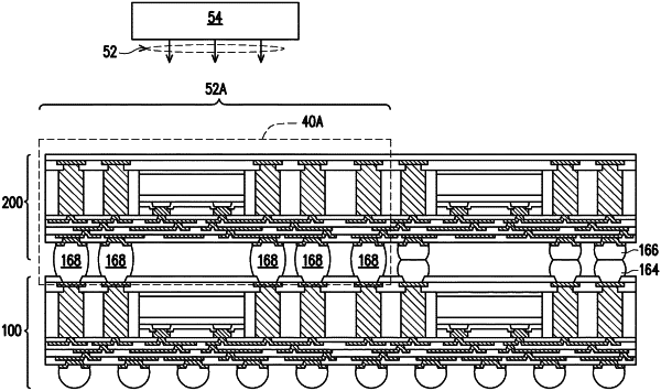
bonding a first package component to a second package component, the first package component comprising first conductive connectors in a first package region and second conductive connectors in a second package region, the first package region adjacent the second package region, the bonding comprising:
projecting a laser beam at a first portion of the first package component until the first conductive connectors reflow, the first portion of the first package component overlapping each of the first conductive connectors and a subset of the second conductive connectors;
turning off the laser beam until the first conductive connectors solidify;
projecting the laser beam at a second portion of the first package component until the second conductive connectors reflow, the second portion of the first package component overlapping each of the second conductive connectors and a subset of the first conductive connectors; and
turning off the laser beam until the second conductive connectors solidify.
|