| CPC H01L 25/18 (2013.01) [H01L 23/528 (2013.01); H01L 24/05 (2013.01); H01L 24/08 (2013.01); H01L 24/09 (2013.01); H01L 24/89 (2013.01); H01L 25/50 (2013.01); H10B 41/27 (2023.02); H10B 41/30 (2023.02); H10B 41/40 (2023.02); H10B 43/27 (2023.02); H10B 43/30 (2023.02); H10B 43/40 (2023.02); H01L 2224/0557 (2013.01); H01L 2224/08147 (2013.01); H01L 2224/0913 (2013.01); H01L 2224/80001 (2013.01)] | 6 Claims |

|
1. A semiconductor device, comprising:
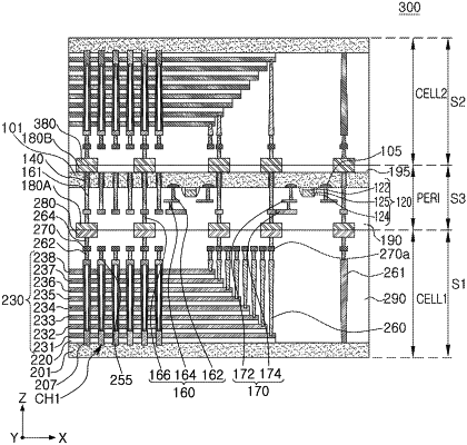
a first substrate structure including a first substrate, gate electrodes stacked and separated from each other in a first direction, perpendicular to a first surface of the first substrate, and extended by different lengths in a second direction, parallel to the first surface of the first substrate, to provide contact regions, cell contact plugs extending in the first direction and connected to the gate electrodes in the contact regions, and first bonding pads disposed on the cell contact plugs to be electrically connected to the cell contact plugs, respectively; and
a second substrate structure, connected to the first substrate structure on the first substrate structure, and including a second substrate, circuit elements disposed on the second substrate and electrically connected to the gate electrodes, and second bonding pads disposed on the circuit elements to correspond to the first bonding pads and bonded to the first bonding pads,
wherein, in the first substrate structure, the contact regions include a first group of contact regions each having a first width in the second direction and a second group of contact regions, wherein for each contact region of the second group, at least a portion of the contact region vertically overlaps at least one first bonding pad, and the contact region has a second width in the second direction greater than the first width, and the second width is greater than a width of the at least one first bonding pad,
the first substrate structure further includes channels passing through the gate electrodes and extending perpendicularly to the first substrate, bit lines electrically connected to the channels, and third bonding pads disposed to be electrically connected to the bit lines,
the second substrate structure further includes fourth bonding pads bonded to the third bonding pads, and
the third bonding pads have a size substantially the same as a size of the first bonding pads.
|