| CPC H01L 23/367 (2013.01) [H01L 21/823821 (2013.01); H01L 21/823871 (2013.01); H01L 23/3171 (2013.01); H01L 23/5226 (2013.01); H01L 23/5283 (2013.01); H01L 23/5286 (2013.01); H01L 27/0922 (2013.01); H01L 28/10 (2013.01); H01L 29/0673 (2013.01); H01L 29/66545 (2013.01); H01L 29/66795 (2013.01); H01L 29/775 (2013.01); H01L 29/7851 (2013.01); H01L 2224/0401 (2013.01)] | 20 Claims |

|
1. A method comprising:
forming a transistor on a semiconductor substrate;
thinning the semiconductor substrate to expose a source/drain region of the transistor;
after thinning the semiconductor substrate, forming a first interconnect structure on a backside of the transistor, wherein forming the first interconnect structure comprises:
depositing a first dielectric layer on a backside of the transistor;
forming a contact through the first dielectric layer, the contact is electrically connected to a source/drain region of the transistor;
forming a conductive line electrically connected to the contact; and
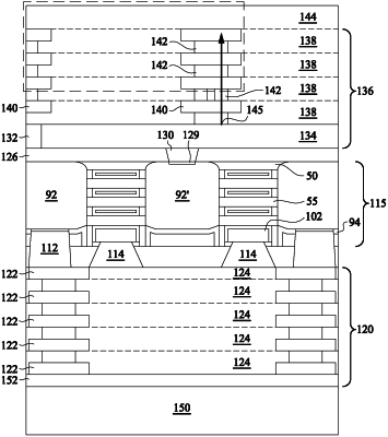
forming a thermal dissipation path from the conductive line to a surface of the first interconnect structure opposite the transistor, wherein the thermal dissipation path comprises a dummy via; and
forming an external connector over the first interconnect structure, the external connector is thermally connected to the conductive line through the dummy via.
|