| CPC H10K 59/1315 (2023.02) [H10K 59/1213 (2023.02); H10K 59/353 (2023.02)] | 17 Claims |
|
1. A display panel, comprising:
a base substrate;
a gate conductive layer on the base substrate, comprising a plurality of scanning lines;
a first insulating layer on the gate conductive layer;
a first conductive layer on a side of the first insulating layer away from the base substrate, comprising a plurality of data lines, wherein the plurality of data lines are arranged in a first direction;
an interlayer insulating layer on a side of the first conductive layer away from the base substrate; and
a second conductive layer on a side of the interlayer insulating layer away from the base substrate, comprising an auxiliary power line; wherein
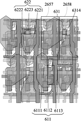
the auxiliary power line comprises: a plurality of sub-auxiliary power lines and a plurality of auxiliary conduction lines; the plurality of sub-auxiliary power lines are arranged in the first direction and extend in a second direction, and adjacent two of at least part of the sub-auxiliary power lines are electrically connected by at least one auxiliary conduction line; the first direction and the second direction are different; and
an orthographic projection of at least one of the plurality of auxiliary conduction lines on the base substrate does not overlap an orthographic projection of the scanning lines on the base substrate;
wherein the plurality of scanning lines comprise first scanning lines and second scanning lines; one second scanning line comprises: a scanning line portion and a plurality of protrusion portions that are electrically connected to each other; the scanning line portion extend in the first direction, and the protrusion portions extend in the second direction;
the display panel further comprises: a plurality of sub-pixels; at least one of the plurality of sub-pixels comprises a pixel driving circuit; the pixel driving circuit comprises a transistor; and
the protrusion portions serve as a gate of the transistor, and an orthographic projection of each of the auxiliary conduction lines on the base substrate does not overlap an orthographic projection of the protrusion portions on the base substrate;
wherein the display panel further comprises: a plurality of repeating elements; the repeating elements comprise the plurality of sub-pixels; the plurality of repeating elements form repeating element rows, repeating elements in each repeating element row are arranged in the first direction, and the repeating element rows are arranged in the second direction;
the auxiliary conduction lines comprise first auxiliary conduction lines; adjacent two of part of the sub-auxiliary power lines are electrically connected by at least one first auxiliary conduction line of the first auxiliary conduction lines;
one repeating element row corresponds to one first scanning line, one second scanning line and at least one first auxiliary conduction line; and
for the first scanning line, the second scanning line and the first auxiliary conduction line that correspond to the same repeating element row, an orthographic projection of the first auxiliary conduction line on the base substrate is between orthographic projections of the first scanning line and the protrusion portions of the second scanning line on the base substrate.
|