| CPC H10K 59/131 (2023.02) [H01L 24/05 (2013.01); H01L 24/06 (2013.01); H01L 24/29 (2013.01); H01L 24/32 (2013.01); H10K 59/90 (2023.02); H01L 2224/05022 (2013.01); H01L 2224/05073 (2013.01); H01L 2224/05124 (2013.01); H01L 2224/05139 (2013.01); H01L 2224/05147 (2013.01); H01L 2224/05166 (2013.01); H01L 2224/0518 (2013.01); H01L 2224/05562 (2013.01); H01L 2224/05571 (2013.01); H01L 2224/05573 (2013.01); H01L 2224/05688 (2013.01); H01L 2224/06152 (2013.01); H01L 2224/29017 (2013.01); H01L 2224/29028 (2013.01); H01L 2224/32145 (2013.01); H01L 2924/0549 (2013.01); H01L 2924/1426 (2013.01)] | 20 Claims |
|
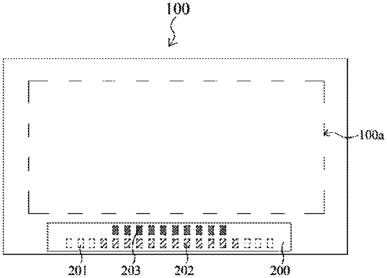
1. A display panel, wherein the display panel comprises a display area and a pad area, and the pad area is disposed on one side of the display area, the display panel comprising:
a substrate comprising a bearing surface;
a first conductive pad disposed on the bearing surface of the substrate, and the first conductive pad is located at the pad area;
a second conductive pad disposed on the bearing surface of the substrate, and the second conductive pad is located at the pad area; and
a driving chip bonded to the pad area, and the driving chip comprising:
a first pin disposed corresponding to the first conductive pad;
a second pin disposed corresponding to the second conductive pad;
a first conductive adhesive layer filled between the first conductive pad and the first pin and electrically connected to the first conductive pad and the first pin; and
a second conductive adhesive layer filled between the second conductive pad and the second pin and being electrically connected to the second conductive pad and the second pin;
wherein a distance from a surface of the first conductive adhesive layer close to the first pin to the substrate is different from a distance from a surface of the second conductive adhesive layer close to the second pin to the substrate; and
wherein the first conductive pad comprises a first bonding surface, the first bonding surface is at least partially parallel to the bearing surface and in contact with the first conductive adhesive layer, the second conductive pad comprises a second bonding surface, the second bonding surface is at least partially parallel to the bearing surface and in contact with the second conductive adhesive layer, and a distance between at least part of the first bonding surface parallel to the bearing surface to the substrate is different from a distance between at least part of the second bonding surface parallel to the bearing surface to the substrate.
|